
A spare block pool and a bad-block table sit behind every flash part, and buyers never see either. This piece separates the two events that share the word 'bad block' — the failures marked at wafer test and the ones that appear in your product — and shows what happens to a unit when the reserve area runs dry.
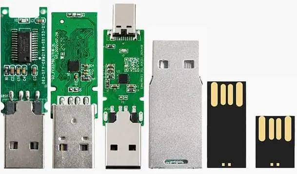
A bad block gets reported the same way whether it failed at the factory or in your product, and the controller treats the two events differently. At the wafer the die is probed, blocks that do not hold a programmed bit are marked, and the pattern is mapped into a reserve area held back behind the advertised capacity. In the field a worn cell flips a bit past the point error correction can repair, and the block is retired into that same reserve. The reserve is finite. Once it empties the part refuses new writes and reports itself as full, which is why an outbound test that only fills the advertised capacity can pass a unit that was built with almost nothing left in reserve. This mechanism is industry behaviour, not our measurement.
A block is “bad” before your product exists, and again later
Field failures arrive reported as one phrase. A camera logs “card error”. A returns sheet says “corruption”. Neither statement says whether the failing block was marked at the wafer or retired after months of writing, because the controller does not tell the host the difference — both end up in the same table inside the firmware.
The two events behave differently enough to plan around. The first is a screening outcome, decided before the die is ever bonded into a module. The second is a consumption outcome, driven by the workload your product actually generates. A buyer who assumes “bad block” always means the second will misread a screening result as a field defect, and a buyer who assumes it always means the first will treat a worn part as if it were brand stock.
The screening case is worth stating plainly. During wafer test the die is probed block by block. Blocks that will not hold a programmed bit are marked and skipped, and the pattern is written into a table the controller keeps. That table is why a part can ship with a known fault count and still hold its advertised capacity.
What the reserve area is for
The NAND die behind the part is never a clean grid, and the industry’s answer is to sell more raw capacity than the part advertises and hold the surplus back. The JEDEC and ONFI NAND interface work describes the spare area and the bad block information at the die level. Above that layer, the decision — how many blocks to hold in reserve, when to retire one, what to do when the pool empties — lives in the controller firmware. The SD Association physical layer specification governs how a TF card presents itself to a host; the USB-IF work governs the module side. Neither publishes a spare-area ratio you can buy against.
That mechanism, and the numbers attached to it, is industry behaviour. It is not a measurement from our own floor, and no figure in this section comes from a test we ran.
What is published and independently describable is the cell budget the reserve draws against. Those are cell-type averages from the JEDEC endurance definitions in JESD47 and JESD84:
| Cell type | Typical program/erase cycles |
|---|---|
| SLC | about 100,000 |
| MLC | about 3,000 – 10,000 |
| TLC | about 1,000 – 3,000 |
| QLC | about 300 – 1,000 |
The spread inside each row is real. It moves with the process node, the interleave the controller can hold, and the temperature the cells sit at. Because managed NAND programs in pages and erases in blocks, the traffic the cells absorb runs larger than the traffic the host asked for — industry figures put write amplification commonly between 8 and 20 times — so the retirement clock runs faster than the raw cycle count suggests.
When a block wears out mid-life
A block does not fail politely. It degrades: the threshold for telling a stored charge apart drifts, reads start returning soft errors, and the controller’s error-correcting code repairs them on the fly. Repaired errors are normal. The point of no return arrives when the code can no longer repair them, or when the block can no longer be erased to a clean state.
At that moment the firmware retires it. The logical address that pointed at the dead block is remapped to a block from the reserve area, the bad-block table grows by one entry, and the host keeps writing without noticing anything changed. That remapping is invisible by design. A part can be deep into its reserve pool and still read and write perfectly.
Invisible is the problem. The host sees correct bytes right up to the moment it does not.
When the reserve runs out
The pool is finite, and the industry does not publish a figure stating how big it is. What happens next is consistent across controllers: the part stops accepting new writes, reports itself as full, and holds whatever data is already mapped. Reads usually keep working. Erase and program status codes start returning failures.
This is the failure mode buyers misdiagnose most often. A unit that suddenly reports “full” with bytes still readable, in a device that overwrites a loop, looks like a host bug. It is frequently a retired-block count that caught up with the reserve.
The arithmetic is what matters. Take a 32GB unit from the TF band our specification cards cover — 4GB to 256GB — assembled on TLC cells at the low end of the published budget, roughly 1,000 program/erase cycles. A device capturing 20GB an hour, with write amplification applied by the controller, will retire blocks on a schedule measured in weeks rather than years. The same capture rate on an SLC part in a read-mostly device never gets there at all.
What an outbound test can and cannot prove
Sampling for outbound inspection follows ISO 2859-1 / ANSI-ASQ Z1.4, with General Inspection Level II as the default when a contract is silent. At Level II a lot of 3,201 to 10,000 units draws a sample of 200, and the acceptance numbers shift with the assigned AQL. That is the right tool for catching a process that drifted that shift.
It is the wrong tool for spotting a unit built with a nearly empty reserve. The only outbound test that takes the part at its word is write-and-read-back: fill the whole advertised capacity, then read every byte back and compare. It catches units whose replacement blocks were mapped outside what the host can address. What it does not do is report the reserve headroom left afterwards, so two units can pass the identical test and have very different lives ahead of them.
That difference is why the test question to ask of a supplier is not “do you test” but “what does the test report”. A fill-and-verify pass record and a reserve headroom count are not the same document.
What we publish, and what we do not
Our three formats are the ones an engineer can check with a caliper and a scale, and they are the only figures we put in front of a buyer:
| Format | Size | Mass | Capacity range |
|---|---|---|---|
| TF card | 15 × 11 × 1 mm | 0.25 g | 4GB – 256GB |
| UDP (USB Disk in Package) module | 11.3 × 24.8 × 1.45 mm | 0.819 g | 128MB – 128GB |
| Semi-finished board | 12 × 44 × 4.5 mm | 3.2 g | 128MB – 128GB |
Read and write speed is stated as customizable per order rather than as a fixed megabyte figure, because the number depends on the controller and die in the build and on the host it is measured in.
We do not publish a spare-area ratio, a bad-block count, a program/erase rating, a TBW figure or a serial-level test report, and we hold no certificate scans we can release. If your engineering file needs one of those documents, ask and we will say plainly whether it exists. We will not produce a document number to end an argument.
Four lines to put in the RFQ
Ask these before the die is chosen, when the change still costs a conversation:
- What is the write ratio of the workload? A logger that rewrites the same 4 kB line every ten seconds retires blocks differently from a camera writing 30MB video segments, and the reserve pool does not care which one you meant.
- What peak ambient temperature will the cells see? Endurance and retention both fall as the cells sit hotter, and a sealed enclosure raises the real number above any datasheet guess.
- What happens when the part stops accepting writes? Get the failure mode in writing. A part that keeps reading data after writes fail is a different product decision from one that dies outright.
- Will reserve headroom be recorded at despatch? If your incoming QC expects to trace a return to a number, the answer is usually no — and knowing that now is cheaper than finding out on an RMA.
The SD Association and USB-IF work will not settle these four for you. They set the interface. The firmware sets the life.
When we are the wrong supplier
Several situations call for a supplier other than us, and saying so here costs less than a tooling order.
If you need a contractual bad-block count per serial number, or an endurance guarantee backed by an independent test report, we cannot produce that document today, so do not place the order on the strength of one. If your requirement is commodity retail flash at the lowest unit price with no marking and no custom configuration, we are not the cheapest source and you should buy from a commodity channel. If your product writes continuously at an elevated temperature and your failure analysis depends on serial-level reserve data, we will not have those numbers and you will need a supplier who instruments that way.
The honest line: if the part you need is defined by a written endurance guarantee, buy from a supplier who can produce the test report behind it. If the part you need is a predictable block of NAND behind a known controller, in a shape that fits, that is what we build.
Ask for the mechanism, not the promise
Bad block handling is not a marketing claim. It is a table inside a controller, a pool of reserved blocks, and an arithmetic limit that your workload reaches on a schedule you can calculate. None of that is visible from the outside until it is too late to change the design.
Put the workload, the temperature and the end-of-life behaviour into the order. What is left — which block the firmware swaps in, and why — is the supplier’s side of the job.
Frequently asked questions
Is a bad block the same thing as a failing cell?
No. A failing cell is one bit or one page that will not hold a charge. A bad block is the controller's classification of a whole block after enough cells in it fail together. One bad block usually costs you a far larger amount of raw flash than one bad cell, because the block holds many pages.
Does a part with more bad blocks at despatch mean worse quality?
Not necessarily. A die that showed many factory-failing blocks is still a working die if the controller mapped all of them into reserved space and the spare pool still has margin left. What matters is the headroom left in the pool, not the count of blocks that were replaced at the start.
Can a brand new card be bad-block-limited?
Yes, when the reserve area was sized close to the fault count of that particular die. This is why two units from the same capacity band and the same order can behave differently in a long write test, even though both passed the same outbound check.
What do the endurance figures have to do with bad blocks?
They set how fast blocks reach retirement. The published program/erase budgets run from about 100,000 cycles for SLC down to 300 to 1,000 for QLC. Every retirement draws on the same spare area, so a QLC part under a heavy write workload reaches the pool limit sooner than an SLC part under the same workload.
Does write-and-read-back testing find bad blocks?
It finds the ones that already affect the advertised capacity. If a failing block was mapped into reserve space before the test ran, the test writes correct bytes to every address the host can see. What the test does not do is count how much reserve was consumed to get there.
Can a buyer specify how large the spare area should be?
Not through the SD Association or USB-IF interface work — neither publishes a spare-area number you can buy against. Ask it as a direct question instead: what reserve ratio the controller is configured with, what the outbound test does at end of life, and whether a unit that stops accepting writes is treated as a defect. A supplier who can answer all three has the firmware in front of them. One who only quotes a warranty year does not.