
A flash order is quoted against a delivery date, but the quantity behind that date was fixed at wafer test weeks earlier. This piece separates the two numbers buyers argue about — the schedule and the die yield — and shows which one a supplier can move and which one cannot.
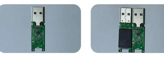
The delivery date on a flash quotation and the quantity behind it come from two different places. The date is scheduling: tooling, assembly, test and packing, which a supplier can re-plan. The quantity that can be scheduled was fixed at wafer test, where each die on the wafer is probed and the ones that fail are marked. That yield is set upstream, cannot be recovered during assembly, and cannot be negotiated after the fact. What a packager can still choose is which wafer lots to open, which die grade to use, and which package format to build into. A buyer who asks about screening weeks before the order lands gets a real answer; the same question asked at the end of a tooling cycle is a complaint, not a lever.
The date on the quote and the number behind it come from different places
A flash order arrives with a delivery date, and most buyers plan around that date as though it were a statement about the supplier’s calendar. The calendar is real. It sits downstream, and it is the part we can actually re-plan — tooling, COB bonding, housing, marking, test and packing.
The quantity that calendar is planning to build was decided upstream, at wafer test, before any of it. A wafer leaves the fab with a yield figure attached to it: the proportion of die on that wafer which survived probing. Assembly cannot add die back. A packager can only choose which lots to open, which die to take from them, and which package format to build.
For a buyer that distinction decides which questions are worth asking, and when.
What happens while the die is still a square on a wafer
During wafer test the wafer is held on a prober and each die is contacted individually through a probe card. Patterns are written into the memory cells and read back. Cells that will not hold a pattern, and blocks where enough cells fail together, are marked on a per-die map.
That map is the die’s report card, and it is written before anyone knows what product the die will end up in. A die carrying too many marks is not automatically scrap. It may be binned out of the high-capacity grade it was built for and still be perfectly good as something smaller, which is the reason two units from the same part number can behave differently in the field and why one wafer can feed two capacity bands in the same week.
Everything in that paragraph is how the memory industry tests wafers, described the way the foundries and test houses describe it. It is not a measurement from our own floor, and no figure in this section is one.
Why the capacity you ask for changes the arithmetic
Screening does not scale with what you buy. A small part is usually one die or a stacked pair. A 256GB unit needs either several die or a single die with a much taller stack — and modern NAND gets that capacity by stacking cells in layers instead of spreading them across the die surface.
On a wafer of fixed diameter, both routes cost something. More die per part means more of them must pass. A taller stack means more process steps where a defect can land, and yield on a stack is the product of the yield of each layer, which is why the top capacities are the first to tighten when upstream demand rises.
The practical consequence is simple: the larger the capacity, the fewer usable die a single wafer yields, and the less room the packager has to substitute when one supplier’s lot disappoints. That is a supply statement, not a complaint about any particular factory.
It is also why the package format matters more than it looks. Our sourcing list covers TSOP, BGA, LGA, COB and eMMC, with die attributed to SanDisk, Toshiba, Micron, SK Hynix, Intel and Samsung, and controller work in QFN, 24-pin, 48-pin and COB formats across four controller solutions. That list is a statement of what we can route around. It is not a promise that any two entries swap places: a BGA part will not drop into a footprint built for TSOP in the last week of a programme.
Where the weeks actually go
The schedule a buyer sees is a slice of a much longer path. The industry cycle figures published for this part of the chain look like this:
| Stage | Typical duration |
|---|---|
| Wafer fabrication | up to 12 weeks |
| Assembly and test | a further 4 to 8 weeks |
| Full path from fab through test and assembly | roughly 26 weeks |
Those are ECIA pipeline figures and component packaging standards, not measurements taken by us. The reel quantities that follow from them are fixed the same way: surface-mount parts ship on carrier tape sized by EIA-481 and IEC 60286-3, so a reel holds 10,000 pieces of a 0402 chip on a 7-inch reel and 50,000 on a 13-inch one, 2,500 for a narrow SOIC-8 and 1,000 or 3,000 for a SOT-23. Those numbers follow from package size and tape pitch. They are not commercial policy, and no amount of order size moves them.
The inventory that sits between those stages has been benchmarked too: roughly 180 days of unpackaged die banked upstream and about 65 days held at distributor level. When an upstream facility has a bad quarter, that buffer is what absorbs it — until it does not.
What we can route around, and what we cannot
Our side of the chain starts after the wafer has done its work. The stages on our floor are wafer sorting and testing, COB bonding or SMT placement, housing and assembly, marking and branding, then test and pack. Everything in that list is a scheduling problem in the sense that a good planner can move it.
The yield above it is not. When a lot opens short, the honest answer is a longer date, not a lower price. Buyers sometimes read that as a negotiation failure. It is the opposite: it is the supplier telling you where the constraint is.
The three form factors we publish carry the only product figures we put in front of a buyer, because they are the ones an engineer can check with a caliper:
| Format | Size | Mass | Capacity range |
|---|---|---|---|
| TF card | 15 × 11 × 1 mm | 0.25 g | 4GB – 256GB |
| UDP (USB Disk in Package) module | 11.3 × 24.8 × 1.45 mm | 0.819 g | 128MB – 128GB |
| Semi-finished board | 12 × 44 × 4.5 mm | 3.2 g | 128MB – 128GB |
Read and write speed is stated as customizable per order instead of a fixed megabyte figure, because the achievable speed follows from the die and controller in that build and from the host it is measured in.
Four questions to put in the RFQ early
- What capacity band is being sized for, and is a lower one acceptable as a fallback? A fallback band that fits the same enclosure converts a shortage into a choice. The same question asked after tooling is already cut has no answer left.
- Which die sources are acceptable, and which are excluded? Naming a maker improves one part of the conversation and removes another. Specifying “any die from the published list, second source pre-qualified” keeps both sides of it open.
- Is a second package format qualified on the same board? TSOP and BGA across the same enclosure is a modest amount of engineering work before volume and an impossibility after it.
- What happens to the date if the opened lot comes in short? A supplier who answers with a mechanism has visibility into their chain. A supplier who answers with a new date has none.
None of these questions creates die out of nothing. They all move the point in the programme at which a shortfall becomes visible, and that is worth more than a week of schedule.
When we are the wrong supplier
Several situations call for someone else, and saying so here costs less than a tooling order.
If your product is pinned to a named fab allocation with a contractual volume, you need a supplier holding a reservation with that fab, not a packager buying lots in the open market. If your board only accepts the die you excluded at specification time, the sourcing list we publish cannot help you and no technique will. If you need a written wafer-yield or die-map report per lot, we do not produce one; ask and we will say plainly whether the document exists rather than produce a number to end an argument.
If what you need is a known controller and a selection of die behind it, in a shape that fits, built by people who can explain where the weeks went, that is what we do. The rest of it belongs upstream, and no supplier can rent it.
Ask about the wafer before the board exists
Screening is a small event with a long shadow. It happens before packaging, before tooling, before the first line of your order is scheduled, and it decides the difference between a date you can plan a launch around and a date you are waiting on.
Put the capacity band, the acceptable die range and the package fallback into the order while the change still costs a conversation. What is left afterwards — which lot opens, which die gets used, how long the assembly takes — is the scheduling half of the job.
Frequently asked questions
Can a supplier recover a low wafer yield later in the process?
Not really. Once a wafer is probed and the die map is written, the unusable die stay unusable. Assembly and test can only decide which of the good die get used, in which product, and in what quantity. If the opened lot was short, the shortfall shows up as a longer lead time rather than as a better price.
Why does the same part number sometimes ship in two weeks and sometimes in eight?
Because the wafer lot behind it differs. Fab runs upstream of us take up to 12 weeks and assembly plus test add a further 4 to 8 weeks, and the full path from fab to test and assembly is around 26 weeks. A lot that already exists in the channel can ship quickly; a lot that has to be started has to wait its turn.
Does the package format change how many dies a wafer yields?
The package does not change the wafer. What changes is how substitutable the result is. A BGA part cannot be dropped into a footprint built for TSOP at short notice, so when one die source tightens, the alternative may exist on paper and not in your board.
Should we specify the die brand in the RFQ?
Sometimes. Naming a maker makes the supply position clearer, but it also removes the second source you may need later. The more useful question is usually whether the specification permits any die from the published list, and what happens if the named one is unavailable.
What can a buyer do when the die yield comes in low?
Three things, all of them cheaper earlier than later: release volume in batches against a standing commitment, agree a second package format that fits the same enclosure, and keep a second controller solution qualified on the same board. None of them creates die out of nothing.
Does WINTEL publish its own die yield or wafer figures?
No, and we do not buy against a published figure for them. What we state publicly is the sourcing list and the package formats, plus the three form factors and their dimensions. Any figure describing someone else's fab belongs to that fab, not to us.