
Wear levelling spreads erases across a NAND die so no single block dies early. This piece separates dynamic from static levelling, shows where the mechanism runs out of room, and gives buyers the five questions to put in an RFQ before a controller is chosen.
Wear levelling is the controller's allocation rule: every write lands in a physical block that has taken fewer erases than its neighbours, and blocks holding data that never change get relocated so their erase budget can be reused. Levelling keeps erase counts even, and that evenness is what turns a published program/erase budget into a product life. The controller sees only the logical write pattern, so a host rewriting the same small region consumes budget at the same rate as a genuine refresh, and a device whose payload is mostly a device image leans on the static half of the mechanism. No published standard fixes the over-provisioning it runs on. This is industry behaviour, not a measurement from our own floor.
The controller is moving your data whether you asked or not
Wear levelling is the firmware job that keeps a flash part alive, and it is the least visible thing inside the device. Its purpose is to leave nothing for a host to inspect. A perfectly levelled part is one where no block looks busier than any other, so no tool, no log and no counter reports anything worth reading.
A purchase spec lists capacity, a speed class and a warranty year. The mechanism that decides how many of those years you actually get is not on the list, and neither the SD Association physical layer specification nor the USB-IF module work publishes a figure you can buy against.
This piece covers what the mechanism does, where it runs out of room, and how to ask for it while the die is still a decision on a call. No parts catalogue. If you only need a shape that fits an enclosure, start with the product pages.
A logical address and a physical block are not the same thing
NAND cannot overwrite a page in place. It programs pages inside a block and erases the whole block at once. Write enough to a flash part and that constraint stops being theoretical. The controller carries a translation layer that maps what the host asks for — a logical sector — onto wherever there is room on the die.
When that logical sector is written again, the controller does not rewrite the old page. It programs a new one elsewhere, repoints the map, and marks the old space free. That indirection is the whole reason a flash part can look like a disk.
Everything below follows from it, and an allocation rule that always dropped each new write into the lowest-numbered free block would spend one block’s whole budget while the rest of the die sat untouched.
Dynamic levelling spreads writes; it cannot read your mind
Dynamic wear levelling sends each new write to a block whose erase count is lowest at that moment. Under an ordinary mix it does its job, and erase counts across the active region stay close together.
What it cannot do is tell what your data means. A host rewriting the same 4 kB line every second produces real traffic, and at that layer the command looks identical to a refresh of new contents: the controller allocates a fresh page and the erase count climbs.
Static levelling is the part that catches buyers out
Dynamic levelling only spreads writes among blocks that are already erased and free. It has no answer for data that never changes. A device image, a firmware file, an archive nobody touches: whichever blocks those occupy sit through the service life taking almost no erases, while every other block absorbs the full workload.
Without static levelling that arrangement quietly concentrates wear on the small share of the die holding the active data. The remedy is to copy the cold data into a block that is due for erasure, free the block it lived in, and let that block rejoin the pool. Relocation runs on a schedule the firmware picks, sometimes while the device sits idle.
A device whose payload is mostly static — a thin client, a kiosk, an appliance storing firmware and settings — leans on this mechanism far harder than a camera does. A short bench test will not show any of it: two hours of writing 20GB leaves the cold blocks exactly where they started.
Write amplification turns a workload into a life estimate
Because the cells program in pages and erase in blocks, the bytes they absorb exceed the bytes the host requested. Industry figures put write amplification commonly between 8 and 20 times. The conversion between that and a lifetime is arithmetic, not a measurement of any particular part:
Total bytes the cells can absorb = rated capacity x program/erase budget Host-write endurance = that product, divided by write amplification
Set it against the published cell budgets — about 100,000 program/erase cycles for SLC, roughly 1,000 to 3,000 for TLC and 300 to 1,000 for QLC — and one host pattern leads to very different outcomes. A TLC part running at 8x spends its budget about eight times faster than its byte count suggests. At 20x it is faster again.
The same published definitions carry the retention figures, and those are what surprise an engineer. JEDEC states about 10 years at 40 C at the start of life and about 1 year at 40 C at the end of life after 3,000 program/erase cycles. A part can be inside its retention window and still out of endurance, and one well inside its endurance window can still lose data sitting too hot.
What is published, and what is not
This section is industry behaviour read from public sources: the JEDEC endurance and retention definitions in JESD47 and JESD84, the NAND interface work from JEDEC and ONFI, and the interface specifications from the SD Association and USB-IF. No figure in this section comes from a test run on our floor, and nothing here is our own measurement.
What the public bodies publish stops at the interface and at definitions. Neither the SD Association nor the USB-IF publishes an over-provisioning ratio, a levelling quality figure or a write amplification number that can go into a purchase order. Over-provisioning — the share of the die held back for garbage collection, relocation and reserve — is a firmware choice made inside the part and it is not disclosed.
That gap is the practical difficulty. Two parts with the same capacity and the same published endurance budget can be configured with different reserve, and reserve is the input the allocation rule works on. The difference appears in no document either party can hand you.
What an incoming test can prove, and what it cannot
The sampling rules are public and worth knowing. Acceptance sampling follows ISO 2859-1 / ANSI-ASQ Z1.4, with General Inspection Level II as the default when a contract is silent. At Level II a lot of 1,201 to 3,200 units draws a sample of 125 and a lot of 3,201 to 10,000 draws 200; acceptance and rejection numbers move with the assigned AQL, running Ac = 3 / Re = 4 at AQL 1.0 on the smaller sample. That is the right instrument for catching a shift that drifted.
For the part itself, the only test that takes the device at its word is write-and-read-back: fill the whole advertised capacity, then read every byte back and compare. On Windows that is H2testw; on macOS and Linux it is f3write followed by f3read. It proves capacity and integrity and nothing about erase counts, so two units can pass it while sitting at opposite ends of their levelling budget.
Ruling out the other route early saves a quarter. A host cannot verify levelling from outside. No published interface requirement forces a flash part to expose an erase counter an application can read, so software calling something “wear level” is usually reading a vendor extension, not a standard field. Put the requirement in the RFQ.
What we publish, and what we do not
Our three formats are the ones a caliper and a scale can check, and they are the only figures we put in front of a buyer:
| Format | Size | Mass | Capacity range |
|---|---|---|---|
| TF card | 15 × 11 × 1 mm | 0.25 g | 4GB – 256GB |
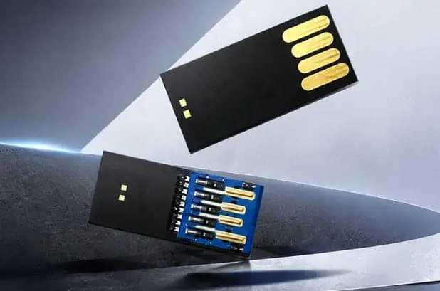
| UDP (USB Disk in Package) module | 11.3 × 24.8 × 1.45 mm | 0.819 g | 128MB – 128GB |
| Semi-finished board | 12 × 44 × 4.5 mm | 3.2 g | 128MB – 128GB |
Read and write speed is stated as customizable per order rather than as a fixed megabyte figure, because the achieved rate depends on the controller and die in the build and on the host it is measured in.
We do not publish an over-provisioning ratio, a write amplification figure, a TBW rating, a program/erase rating or a serial-level wear report, and we hold no certificate scans we can release. If your engineering file needs one of those documents, ask and we will say plainly whether it exists. We will not produce a document number to end an argument.
Five lines for the RFQ
- What share of the die is held back as over-provisioning? Ask for a number. A supplier who says “it depends on the controller” has told you it is not documented anywhere.
- Is static levelling enabled, and does it run at idle? A device with a static payload needs this more than a camera does.
- What is the workload’s write ratio? A logger rewriting the same 4 kB line is not equivalent to a camera writing 30MB segments.
- What retention does the part need at our enclosure temperature? The published retention figures are stated at 40 C. A sealed housing moves the real number up.
- What does the part do at end of life? Get the failure mode in writing. A unit whose blocks are exhausted does not behave like one whose cells have simply worn past retention.
None of those five come from a standard. The standards set the interface; the firmware decides the life.
When we are the wrong supplier
Several situations call for another source, and naming them here costs less than a tooling order.
If your requirement is a written TBW or endurance guarantee backed by an independent test report, we cannot produce that document today, so do not commit on the strength of it. If you need serial-level erase counters exported per part for field failure analysis, we do not record them, and a supplier who instruments that way is the right starting point. If you want commodity retail flash at the lowest unit price with no marking and no custom configuration, buy from a commodity channel — we are not that, and you should not expect us to be.
The honest line: if the part is defined by a written endurance guarantee, buy from whoever can produce the report behind it. If it is a predictable block of NAND behind a known controller, in a shape that fits, that is what we build.
Levelling works, which is exactly the difficulty
The mechanism is good at its job and silent about it. A part can be perfectly levelled and still finish its life early, because the workload it saw was heavier than the published figures assume. None of that shows up in a bench test, a speed class or a warranty year.
Put the write pattern, the cold-data share and the enclosure temperature into the order while the die is still a decision on a call. What is left — which block takes the next erase — is the supplier’s side.
Sources
Frequently asked questions
Can a buyer ask for wear levelling to be turned off or made more aggressive?
Not through any published interface. The allocation policy sits in the controller firmware and the over-provisioning share is configured there, so the SD Association physical layer specification and the USB-IF module work will not settle it for you. The only route is a direct question to the supplier about the configured ratio and whether static relocation runs at idle. A supplier who has the firmware in front of them answers in numbers; one who answers 'it ships as standard' has not opened it.
Does a larger capacity part levell better than a smaller one?
More blocks give the algorithm more granularity, which helps. The share of capacity held back as over-provisioning matters more than the raw size, and over-provisioning is a firmware choice rather than a published figure. A 64GB unit with a small reserve can age worse than a 32GB unit from the same die family with a larger one.
Why do two identical specs in the same family behave differently in service?
Because the erase budget is consumed by the workload, not by the calendar. A camera writing 30MB video segments and a kiosk holding a firmware file plus a log will both pass the same outgoing test and reach end of life at very different times. Same part, same capacity band, different traffic.
What does write amplification have to do with levelling?
It is the conversion between what the host asks for and what the cells absorb. Industry figures put write amplification commonly between 8 and 20 times, because data is programmed in pages and erased in blocks. Divide the capacity times the program/erase budget by that factor and you have a host-written lifetime, which is the only number your firmware can plan against.
Will H2testw or f3read tell me the erase counts?
No. Fill-and-verify tools prove that the advertised capacity holds its bytes and that nothing was silently stolen from the host's view. They report nothing about how evenly erases are spread, because erase counts are not exposed. A unit can pass both tools with a badly skewed distribution and no symptom.
Does levelling change read performance?
It can, in the form of jitter rather than a lower average. Background relocation copies live data from a block that is due for erasure to a fresh one, and a read that overlaps a copy waits on that copy. On a sustained read you mostly see it as occasional stalls; on a file that is copied once and read forever you see nothing.