A mechanical engineering view of flash storage selection — what 1mm, 24.8mm and 3.2g actually cost you in enclosure design, and how to pick a footprint before you draw the shell.
TL;DR
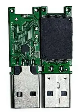
Three flash footprints, three different enclosure problems. A TF card (15 × 11 × 1 mm, 0.25 g) costs you almost nothing in board space but forces a slot into your housing. A UDP module (11.3 × 24.8 × 1.45 mm, 0.819 g) disappears into the PCB stack but locks the storage to the board revision. A semi-finished board (12 × 44 × 4.5 mm, 3.2 g) is the largest, and buys you a known-good PCBA without running your own SMT line.
Pick the footprint before you draw the shell. Reverse-engineering an enclosure around a storage decision made too late is how tooling budgets double.
The three footprints in one table
| Format | Envelope | Weight | Capacity range | What the enclosure must provide |
|---|---|---|---|---|
| TF card | 15 × 11 × 1 mm | 0.25 g | 4GB – 256GB | A slot: insertion depth, ejection, access opening |
| UDP module | 11.3 × 24.8 × 1.45 mm | 0.819 g | 128MB – 128GB | Nothing visible — it lives on the PCB |
| Semi-finished board | 12 × 44 × 4.5 mm | 3.2 g | 128MB – 128GB | A cavity, standoffs, and a USB cutout |
Read the last column again before the spec sheet. Two of these ask the enclosure for something; one asks the PCB. That single distinction drives more enclosure redesigns than any capacity figure.
What the dimensions actually constrain
Enclosure design does not care about gigabytes. It cares about four things: profile height, insertion direction, mounting, and service access. Each format answers those four questions differently.
Profile height. The card’s 1 mm body is thinner than most sockets that hold it, so on a card-based design the socket — not the card — sets your Z-height. The module’s 1.45 mm sits directly on the board, so it competes with every other component for the same vertical space. The semi-finished board, at 4.5 mm, is a stack in its own right: you are housing a finished assembly, not a component.
Insertion direction. A card goes in perpendicular to the PCB in most layouts, which means your housing needs a opening on one face, aligned to the slot. Modules have no insertion at all. The board’s USB port points wherever you routed it — which is an advantage only if you decided it before the shell.
Mounting. Cards are retained by the socket’s spring contacts. Modules are reflowed to the board, so the enclosure never mounts them — it mounts the board they sit on. The semi-finished board needs standoffs or a groove, and its 3.2 g is light enough that adhesive alone is tempting. Resist that temptation in anything that ships in a vehicle or gets dropped; a board bonded with adhesive fails at the bond line, not at the solder.
Service access. Only the card is replaceable in the field. That sounds like an advantage until you count what it costs: an opening, a door or a gasket, and a tolerance chain from the outer wall to the slot. A sealed design with a soldered module has none of that, and its enclosure is measurably cheaper to tool.
The 1 mm problem: a card is a slot decision, not a board decision
The most common sequencing mistake we see is treating the card as a component choice and discovering late that it was an enclosure choice. The card body is 1 mm thin, but the mechanical commitment is the slot:
- Insertion depth. The slot must accept the full card, with tolerance for the user pushing it slightly too far.
- Ejection travel. Push-push or push-pull mechanisms need travel room inside the housing.
- Finger access. Someone has to be able to grip the card to pull it out, or the slot needs an ejection mechanism.
- Label window. If cards are printed with logos or capacity marks, the housing either shows the label or hides it — a branding decision that lands in the mechanical drawing.
None of these are on the card’s datasheet. All of them are on your tooling quote.
The 24.8 mm problem: modules trade access for board real estate
A UDP module is 24.8 mm long and 11.3 mm wide, mounted flat on the PCB. It asks nothing of the housing — and everything of the layout. On a small board, 24.8 mm of length is a corridor you cannot route through. On a large board it is nothing.
The decision is therefore board-shaped, not housing-shaped:
- Small boards (sensors, dongles, adapters): the module’s footprint is the dominant claim on space. Place it first, route around it.
- Large boards (controllers, gateways, industrial PCs): the module is noise. Choose by thermal and service considerations instead.
- Boards with a metal shield: the module goes under it, and the 1.45 mm profile joins the stack-up height budget.
The interface is decided by the controller solution on the module — USB2.0 or USB3.0 — and that choice propagates outward: a USB3.0 link wants shorter, cleaner routing than a USB2.0 link, which is a layout constraint long before it is a marketing one.
Weight is a proxy for what you are actually housing
0.25 g, 0.819 g, 3.2 g. The tenfold spread across the three formats is not trivia; it tells you what the enclosure is holding.
A 0.25 g card is a passive object in a socket. The socket does the work.
A 0.819 g module is soldered mass on a board. Vibration loads it through the solder joints, which is why module-based designs care about board support near the module, not about the housing.
A 3.2 g semi-finished board is an assembly with its own connectors and its own flex. It is the only one of the three where the enclosure is asked to be a chassis. Standoffs, a groove, or a clip are all fine; free-floating adhesive is not.
Which one your enclosure can actually take
Work the questions in this order, and one format usually eliminates itself:
- Is the housing sealed? If yes, the card’s slot is a gasket problem you probably do not want. Module or board.
- Is the PCB already drawn and crowded? Then the 24.8 mm module corridor question answers itself. If there is no corridor, the card (via a slot on the housing face) or the board (as a separate assembly) remains.
- Do you run your own SMT line? If yes, the module is natural. If no, a semi-finished board hands you a populated PCBA without that capability.
- Does anyone ever need to swap the storage? If yes and the answer is final, accept the slot and design for it honestly.
When none of the three footprints fits
Being straight about the limits, because an enclosure rework costs more than a lost order:
- You need storage thinner than 1 mm or smaller than the card envelope. None of the three goes below the card’s profile. That is a bonded NAND or eMMC conversation, not a card one.
- You need more than 128GB in a soldered format. UDP stops at 128GB. Beyond that, the card’s 256GB ceiling is the only path — and it brings the slot back.
- Your housing face has no room for a USB cutout or slot opening. Then the storage has to be internal and soldered, which is the module — but only if the board has the corridor.
- You want a card slot and a sealed housing. Those two requirements fight each other. One of them has to lose, and it is cheaper to decide which one now.
If one of those describes your project, say so at the start. We would rather redirect you to the right format before a quotation than after a tooling revision.
What to send before the enclosure drawing is released
- The housing’s available cavity — internal dimensions and wall thickness, even as a sketch.
- The board outline, if it exists, and where the USB port must land.
- Whether the housing is sealed, and against what (dust, splash, immersion).
- The capacity you actually need — 4GB to 256GB on card, 128MB to 128GB on module or board.
- Service expectation — will anyone open this product after it ships?
With those five lines, the format decision takes minutes and the enclosure design starts on the right footprint. Without them, the storage decision gets made by whoever draws the shell last — which is the most expensive way to make it.
If you are designing a housing now, send the cavity sketch and the board outline. We will tell you which of the three footprints fits before you commit the tooling.
Reach the team at cathy@go-wintel.com or open the request a quote form.
Frequently asked questions
How thick is a TF card and what does that mean for my enclosure?
A TF card is 15 × 11 × 1 mm and weighs 0.25 g. The 1 mm profile means the card itself takes almost no Z-height, but the socket it sits in typically does — the slot, not the card, is what your enclosure has to swallow.
What are the dimensions of a UDP module?
WINTEL's UDP (USB Disk in Package) module measures 11.3 × 24.8 × 1.45 mm and weighs 0.819 g, with capacities from 128MB to 128GB. It mounts directly to the PCB, so the enclosure never sees it — only the board stack-up does.
When would I use a semi-finished board instead of a card or module?
When you want a known-good populated PCBA inside your own housing. At 12 × 44 × 4.5 mm and 3.2 g it is the largest of the three, but it removes the need for you to run an SMT process.
Do I need to reserve space for a card slot in my housing?
Yes, and the slot needs more than the card's 1 mm profile: insertion depth, ejection travel and a finger access opening. If your housing is sealed or too thin for that cutout, a soldered module is the mechanically honest choice.
Can I decide the storage footprint after the enclosure is designed?
You can, but every change after the shell exists is a tooling change. The card, module and board differ in profile, mounting and service access, so the footprint should be fixed before the enclosure drawing is released.
Does capacity affect the footprint?
Within one format, no. A TF card runs 4GB to 256GB in the same 15 × 11 × 1 mm body, and UDP modules run 128MB to 128GB in the same module outline. Capacity changes the die and controller inside, not the envelope your enclosure has to fit.