
Die-level screening is one of three separate test layers in flash memory, and suppliers use the phrase to mean different things. This piece separates wafer probe, incoming die grading and finished-unit testing, states which layers WINTEL runs in Shenzhen, and shows buyers how to verify each claim.
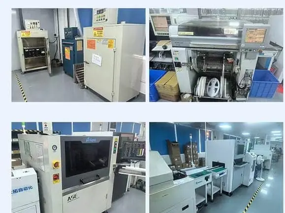
WINTEL performs die-level screening and grading in-house at its Shenzhen plant, as the first of five manufacturing stages. That is distinct from wafer-level probe testing, which runs upstream at the fab or a specialist test house and produces the die map before WINTEL receives the material, and from finished-unit testing, which runs on our line after assembly. A supplier's screening claim is only useful once it says which of those three layers it actually operates. Buyers should ask who contacts the die, who assigns the grade, and what test each layer proves, then match the answer to the documented process rather than to the phrase on the quotation.
Three layers of screening, three different answers
A buyer asking which factory performs die-level screening is usually asking one of three different questions, and the answers come from three different places. The wafer is probed at the fab or a specialist test house. The incoming die is sorted and graded by the packager. The finished unit is tested by whoever assembled it. Those layers get collapsed into one phrase in most supplier conversations, which is exactly why the phrase tells you so little until somebody separates it.
I spend a fair part of each week on calls where this matters. A customer has had a batch fail in the field, or is about to place a first order, and wants to know whether the supplier in front of them controls the part of the process that decides reliability. The honest answer is almost always that we control some of it. The useful question is which part.
What the wafer-level probe establishes
The first layer happens before any packager sees the material. A wafer is held on a prober and each die is contacted through a probe card. Patterns are written into the cells and read back, and the sites that fail are marked on a per-die map. That map is the die’s first report card, and it is written before anyone knows which product the die will end up in.
We do not operate that step, and we do not re-issue its output as a WINTEL measurement. The silicon we source is attributed to SanDisk, Toshiba, Micron, SK Hynix, Intel and Samsung, and the probe history behind a given lot belongs to those makers or to the test house they used. When a supplier shows you a die map and calls it their own test data, the first thing worth checking is who actually contacted the die.
That distinction is not a hedge. It is the difference between a factory that can explain its chain and a factory that is borrowing someone else’s evidence.
What our die-level screening line does in Shenzhen
The second layer is the one we run. Incoming die is screened and graded at our Shenzhen plant before it is bonded or packaged, and it is the first of the five stages we publish for our manufacturing process: wafer sorting and testing, COB bonding or SMT placement, housing and assembly, marking and branding, then test and pack. Grade decided here is the input to everything downstream, because it sets which product the die is fit for and what behaviour the buyer should expect in the field.
That grade is a screening result, not a marketing tier. It records how much testing stood between the die and your order, and it drives retention and failure rate far more than it drives a benchmark number. The practical consequence is that a part which tests fast on the bench can still be the wrong grade for a dashcam writing for hours in a hot car.
We state sourcing and grade per order rather than publishing a catalogue default. That is the only version of the claim I am willing to put on a quotation, because a grade that cannot be tied to a specific build is a grade nobody has to honour.
Three layers, three different proofs
The fastest way to end the confusion is to put the three layers in one table and ask a supplier to mark which ones they personally operate. The answer usually narrows the field immediately.
| Layer | Who runs it | What it proves | What it cannot prove |
|---|---|---|---|
| Wafer-level probe | Fab or specialist wafer test house | Which die sites passed cell pattern test at wafer stage | Final packaged behaviour, field retention, or speed in your host |
| Die-level screening and grading | WINTEL, on our Shenzhen line | Grade and source of the incoming die, and which product it is fit for | The original fab’s process yield, which is upstream of us |
| Finished-unit testing | WINTEL, after assembly | Capacity, reader recognition and write behaviour of the unit shipped | The untouched wafer history, which no downstream test can recreate |
A supplier who claims all three without naming where each happens is describing an ambition, not a process. A supplier who can place themselves in this table has thought about the chain, and can usually tell you where a failure would have surfaced.
Five things a screening claim must name
The KGD and screening concepts have formal definitions in JEDEC documents, including JESD49B.01 and JEP121B. Those are reference frameworks for writing a specification, not certifications held by a commercial flash packager, and we do not present them as a mark on our products. Their value to a buyer is the discipline they impose on the question.
That discipline reduces to five things worth putting in writing before an order.
| Item to fix | What to ask the supplier | What a real answer sounds like |
|---|---|---|
| Layer ownership | Which of the three test layers do you operate yourself | We screen and grade incoming die and test finished units; wafer probe is upstream |
| Die source | Which makers are on the approved list, and is a second source allowed | Six named sources, with substitution rules stated per order |
| Grade basis | What decides the grade assigned to this build | Incoming screening result tied to the lot, not a catalogue label |
| Document scope | Which reports you issue and which belong to an upstream party | Our test summary plus whatever the fab releases, clearly attributed |
| Failure path | What happens if a lot fails incoming or finished test | Hold, report and agree disposition before the batch moves |
Two columns of adjectives will not survive a batch failure. These five lines will, because each one has an owner and a point at which it can be checked.
Why grade beats benchmark speed in the field
The reason buyers care about who screened the die is not academic. Grade decides how a unit behaves after weeks of use, while benchmark speed decides how it looks in a five-minute test. Those two numbers frequently point in different directions.
A die that was lightly screened can hold a high sequential read figure on day one and still lose retention under sustained write and heat. A die with a stronger screening history may show a more ordinary benchmark and keep behaving the same in month six. For an application that writes continuously, the second part is the one that protects your return rate.
This is also why capacity matters to the screening conversation. A 256GB part needs several die or a taller stack, and a stack multiplies the process steps where a defect can land. The larger the capacity, the fewer usable die a wafer yields and the less room a packager has to substitute when a lot disappoints. Grade and source are not abstract paperwork at that end of the range; they are the supply position.
Three specifications to fix before the order
A die-screening question is only worth asking early enough to change something. These are the three points I ask customers to settle while the design is still open.
First, the capacity band and an acceptable fallback band that fits the same enclosure. A fallback turns a short lot into a choice rather than a delay. Second, the die source list and whether a named maker is required or any source from the published list is acceptable, with a pre-qualified second source. Third, the grade basis and the document you want to see before release, sent at RFQ stage so we can confirm whether it exists.
The three form factors we publish carry the only product figures we put in front of a buyer, because each is a number an engineer can check with a caliper:
| Format | Size | Mass | Capacity range |
|---|---|---|---|
| TF card | 15 × 11 × 1 mm | 0.25 g | 4GB – 256GB |
| UDP module | 11.3 × 24.8 × 1.45 mm | 0.819 g | 128MB – 128GB |
| Semi-finished board | 12 × 44 × 4.5 mm | 3.2 g | 128MB – 128GB |
Read and write speed is specified per order, because the achievable figure follows from the die, the controller and the host it is measured in. Our baseline is 50 pieces per design on standard products, and daily output runs above 20,000 pieces, so the same screening and test sequence applies whether you are releasing a sample run or scaling a volume order.
When we are not the factory you need
There are orders where this answer should end the conversation. If your product is pinned to a named fab allocation under contract, you need a supplier holding a reservation with that fab, not a packager buying lots in the open market. If your specification requires a die map issued by us for someone else’s wafer, we do not produce that document and will not invent a number to close the argument. If your programme needs the original wafer probe performed to a documented military or space standard, that belongs to a test house operating to those frameworks, not to a commercial flash line.
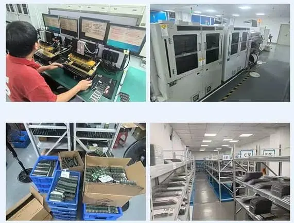
What we can put on the table is a plant that screens and grades incoming die, builds it into TF cards, UDP modules and semi-finished boards, tests the finished unit, and tells you at which of the three layers each fact was established. That is a narrower claim than “we test everything,” and it is one we can stand behind when a batch comes back.
If that is the level of detail you want from a supplier, send the application, the capacity band and the document format you need. We will answer with the grade and source behind your build and the process that produced it, before tooling starts rather than after a failure.
Open the request a quote form or write to cathy@go-wintel.com. You can also see the process itself on the manufacturing page and the products it feeds: TF cards, UDP modules and USB drives.
Sources
Frequently asked questions
Does WINTEL perform die-level screening in its own factory?
Yes. Incoming die is screened and graded at our Shenzhen plant before it is bonded or packaged, as the first of five manufacturing stages. That statement is about incoming die handling on our line; it is not a claim that we operate a wafer fab or perform the original wafer-level probe test.
Who does the wafer-level probe test then?
That happens upstream, at the fab or a specialist wafer test house, before the material reaches us. It produces the die map that records which sites passed. We do not publish or re-issue that map as our own measurement, and we will say plainly when a document belongs to an upstream supplier.
What does die grading actually decide?
Grade decides field behaviour far more than it decides benchmark speed. Retention and failure rate follow the grade, because the grade records how much screening stood between the die and your product. A part that benchmarks well on day one can still be the wrong grade for a write-heavy field application.
Can I request a screening report for my order?
Ask what exists before assuming a format. We state sourcing and grade per order and we run our incoming screening and finished-product tests on our line. A document describing someone else's fab or wafer probe belongs to that fab. If you need a specific report format, send it at RFQ stage and we will confirm whether it can be produced.
Do the JEDEC KGD standards apply to a commercial flash order?
JESD49B.01 and JEP121B give the industry a precise vocabulary for known-good die and for screening optimization. They are reference frameworks, not certifications that a commercial flash packager holds, and we do not present them as a mark on our products. Their value to a buyer is the discipline of asking which layer was screened to what level.
How does this affect minimum order quantity?
Our baseline is 50 pieces per design on standard products. Screening and grading apply to the die lot behind that order, not to a separate service you buy by the wafer, so the same baseline holds whether the order is a sample run or a volume release.